Filename : TOD2.ASC
April 20, 1994
Jerry Decker
KeelyNet
Dear Jerry,
The enclosed copy is to keep you up-to-date on my activities with
regard to the capture of 'space energy'.
I started my work on the Bearden switching circuit in order to be
prepared when the critical semiconductor material is made available.
By much trial and error, my discovery, not invention, is only a
small introduction.
The content of the enclosed contains important correction and update
of my earlier releases.
Please call if there is any question or you would like an updated
complete copy of the circuit and description.
Sincerely,
Lee Trippett
3/20/94
Hal Fox, Editor
New Energy News
P.O. Box 58639
Salt Lake City, UT 84158
Dear Mr. Fox,
Thanks to the advice of Dan Davidson, I recently went to Santa Maria
and met Walt Rosenthal. I have personally experienced the quality
of this man's experience and his reputation for being the final
authority on electrical and electronic measurements. With his
modern and high-tech equipment, he patiently and meticulously
checked every point of data on my version of Bearden's theoretical
switching circuit. (See "Current News on Current Gain", New Energy
News, Feb. '94, p.15.)
Every one of his measurements validated my data. In conclusion,
however, the circuit effects a large current gain but there was no
power gain. Walt's current probes and high resolution test
equipment were able to measure the input power during the short
pulse of the primary circuit. When this measured power is averaged
over the period of the complete cycle, it matched my calculations.
My calibrated analog dc milliammeters represented a true average
current value and so they represented the corrected ON time of the
primary circuit. My error was to apply ON time adjustment to the
"potential" source when the average measured current already
contained, in effect, that adjustment.
There are still rays of hope. Some "space energy" theory relates
directly to this circuit and its present performance. (See
supplement.) A couple of experienced "space energy" researchers
are puzzled by the circuit's non-conventional features. I and
others have gained much experience and knowledge. By the content of
this letter, the two supplements, and past correspondence (see also
KeelyNet files TOD*.*.), my "gain" has been fully shared with many.
When the required 'special semiconductor material' shows up, many
more people will now have an easier time in checking out Tom
Bearden's theory, method #2.
In the meantime, there is still much to learn. Why does this simple
circuit perform as a current amplifier? Why is the current
discharge so incredibly slow for an extremely low circuit
resistance? Why is there so little variation in the performance of
the circuit when the coil "collector" parameters are adjusted over a
wide range? Why is the high current gain limited to a small range
of on-off ratio and frequency? Why does the circuit not work with a
variety of power MOSFETs, even when listed by NTE as equivalent?
Thanks for your vote of confidence by publishing my earlier
experience with the Bearden circuit. It strikes me as a remarkable
coincidence that the coverage of space energy and a preliminary
investigation of Bearden's free energy circuit were in the same NEN
newsletter, and exactly one year after the release of Bearden's
"The Final Secret of Free Energy".
There is still a need to test the circuit with Bearden's mysterious
"degenerative semiconductor material" in the 'collector'. I have
found a source of gold ribbon alloy with 12% germanium. There is
another source for anodized aluminum foil for testing a capacitor
'collector'. Neither source is willing to provide enough sample for
test and the minimum order for both sources far exceeds my limited
budget.
I will keep you posted. Please let me know if there are any
questions.
Sincerely,
Lee Trippett
       cc: Tom Bearden      Dan Davidson
           Jerry Decker     Bill Herzog
           Ed Johnston      Lester Larson
           Dave Marsh       Alexander Peterson
           Chris Terraneau  Ben Trippett
           Dave Trippett
Inc: Space Energy Theory and Replication
The Bearden Circuit and the
View of "New Energy News" on Space Energy
I believe space energy characteristics are behind Bearden's simple
"free energy" switching circuit. Here are some NEN comments on
space energy which relate to my current version of Bearden's
theoretical switching circuit. All references are from the Feb.
'94 issue of New Energy News.
Space energy is fundamental in stabilizing all matter (pg. 3, col.
2, para. 1) and is all-pervading without regard to temperature or
vacuum. (pg. 4, col. 1, para. 4; col. 2, para. 3) It is from "zero-
point fluctuations of the background vacuum electromagnetic field".
(pg. 3, col. 1, para. 3)
Space energy can be tapped without limit (pg. 4, col. 2, para. 3)
from an accelerated frame of reference. (pg.9, col. 1, para. 2)
Electric current through a coil exhibits an aligning effect upon
space energy. The process of modifying the alignment of space
energy couples space energy into electrical coil thus inducing an
electric current. Electric induction can therefore be attributed to
changes in the alignment of space energy. (pg. 9, col. 2, para. 1)
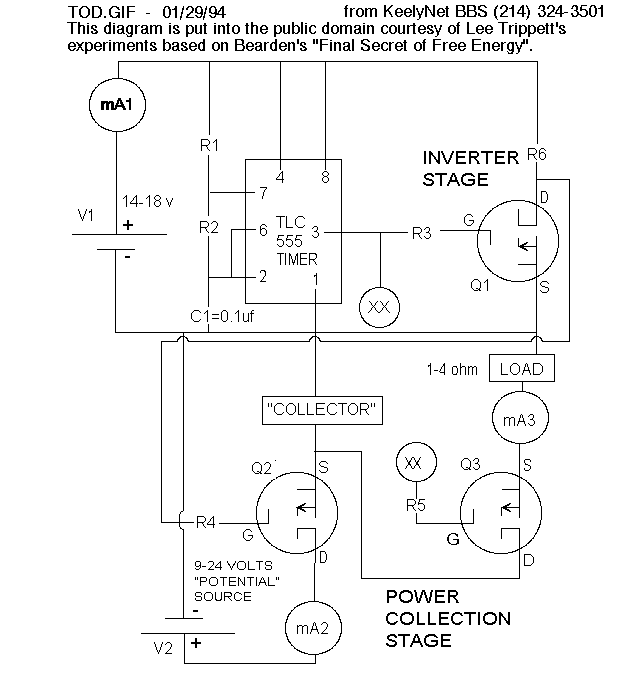
Solutions for Measurements and Replication
This version of Bearden's switching circuit presently shows very
little power capacity but a significant current gain (now up to
200). This is without the use of semiconductor material or the use
of a super high speed switching rate, i.e, 10E-19 sec. And so we
are only at the beginning of our potential! Even though there is
presently a small current in the primary loop (the ideal is none),
the switching circuit demonstrates a large current gain when there
is a sharp pulse (at least on the trailing side), a switch ON of a
few microseconds to a wire "collector", and a low circuit resistance
in both the primary and secondary loops. The "collector" needs to
be at least 30 feet of 22 gauge. Longer and larger is okay.
The ideal measurement tool is a low level DC current probe and a
digital scope. When using series in-circuit milli-ammeters, they
need to have less than 2.0 ohms internal resistance. These are not
common. And so add a shunt to quality low level m icro or milli-
ammeters. However, low resistance DC ammeters have difficulty
reading the low current values in the primary loop. Determining
these low values is critical for proper calculation of gain.
Caution: A pulsed DC current is not the same thing as an AC signal.
Many RMS meters are for common AC or AC on DC patterns. Many
digital ammeters do not take a fast enough sample or take enough
samples to integrate a one microsecond pulse that is ON only 0.2 of
1 percent of the time. A little arithmetic and a simple series DC
circuit with an electronic switch will provide ample demonstration.
Start with a low frequency and an ON OFF ratio of one. Apply the
meters and gradually increase the frequency and then gradually
increase or decrease the ON OFF ratio. This will verify and provide
a calibration for the meters.
When there is a very short ON time of a DC pulse relative to a long
OFF time and when the values are very low on the scale, an extreme
ON OFF ratio can factor a major significance in determining current
or power gain. However, the meter scale can be calibrated by
substituting a known resistor in the "collector" position. The
fixed and known voltage of the Bearden circuit primary loop divided
by the resistor value times the ON/(ON+ OFF) time will establish the
correct current value for the scale.
Calculation of power out is by the current squared times the load
because the high impedance of voltmeters prevents them from
providing an average value with the same relative reference. Low
resistance analog electromechanical DC ammeters can provide a
reasonably accurate average current value.
This is proven by the
meters indicating the same current in both loops when using a
capacitor "collector over a wide range of frequency and ON OFF
ratios. This is also proved by a consistent battery time-energy
drain curve for the same wide range of frequencies and ON OFF
ratios. This is for the situation of a load in the secondary loop
when compared to the same load on a direct battery connection.
However, there is a limit and be sure to note the caution above.
In addition to measurement problems, the lack of replication of a
current gain appears to stem from substituting components with high
internal resistance, slow switching rate capability, or not matching
impedance to maintain a sharp pulse. Even a small signal general
purpose high frequency FET in only the inverter stage degrades the
performance. There are chips and boards especially designed for
driving power MOSFETs. And still yet to be tested are those power
MOSFETs which have a hundred times less internal resistance.
A recent KeelyNet file called ZPETEST offers additional insight and
improvements. (KeelyNet is a free BBS, datum 214-324-3501.) This
file suggests my circuit is similar to a conventional flyback
converter. The circuit is similar but not equal. There is no
evidence of current or voltage leaking from either of the batteries
into the load.
The circuit will support additional parallel "Bearden portions" with
practically no additional burden on the switch and inverter stage.
Questions?
Why does this simple circuit perform as a current amplifier? Why is
the current discharge so incredibly slow for an extremely low
circuit resistance? Why is there so little variation in the
performance of the circuit when the coil "collector" parameters are
adjusted over a wide range? Why is the high current gain limited to
a small range of on-off ratio and frequency? Why does the circuit
not work with a variety of power MOSFETs, even when listed by NTE as
equivalent?

                              February 15, 1994

                                  ZPETEST.ASC
     --------------------------------------------------------------------
          This file shared with KeelyNet courtesy of Chris Terraneau.
     --------------------------------------------------------------------

                ZPETEST.ASC  Zero Potential Energy Test Circuit

           by Chris Terraneau                       9 February 1994

             A number of KeelyNet callers have been experimenting with
             various circuits trying to tap the Zero-Potential energy. I
             have personally designed and built many conventional
             Switching Power Supplies which utilize circuits similar to
             those described in TOD.ZIP and COILBAK.ZIP.

             Several KeelyNetters have initially reported greater than
             unity outputs, only to realize later that some measurements
             may have been done in a manner which obscures what's really
             happening.

             I want to alert everyone to the fact that basically, what
             you MIGHT be actually building is called a FLYBACK
             CONVERTER, Figure 1. In conventional (less than unity)
             circuits, a switch (FET1) is closed for a period of time.
             Current ramps up in the inductor L1, as does the increasing
             magnetic field.

             At some point, FET1 is turned off. The collapsing magnetic
             field in inductor L1 causes a reversal of polarity in the
             voltage across it. This reverse voltage can easily be 10 to
             20 times the input voltage to the circuit.

             What is important to note here is that although the circuit
             has increased the VOLTAGE several times, it has DECREASED
             the current. An INCREASE in VOLTAGE is not the same as an
             INCREASE in POWER if the current has fallen. (P = E x I).

             In some of the circuits I have seen posted here,
             experimenters are advised to use a voltmeter to read a pulse
             voltage. This does not work ! A very GOOD oscilloscope is
             ESSENTIAL if you're going to determine power in a pulse
             circuit where P = E x I x T, where T is Time. Use a 'scope
             with AT LEAST 100 MHz bandwidth.

             It would be far easier to store these 'spurts' of
             voltage/current in a capacitor, and then measure the DC
             output power. If a large enough capacitor is used, T can be
             ignored completely (at least as far as measuring output
             power is concerned).

             Further, FLYBACK-produced current is NOT what you're after !
             A reverse voltage, which is typical of flyback output,
             indicates that you have STORED energy in an INDUCTOR in its
             MAGNETIC FIELD.

             Fig. 1 - Typical FLYBACK Converter

                                 + V
                                    |
                                    |
              (+)          (-)      |
                                   C
            FET1 ON      FET1 OFF  C
           (charging)   (flyback)  C   L1
                                   C
              (-)          (+)      |
                                    |
                                    +--------------- OUTPUT PULSE
                                    |                see waveform below
      ___________                   |
     |           |                  |
     |           |                  | D
     | Drive     |-------------] [--+
     |           |         G   ]        FET1
     |   Circuit |             ] [--+
     |           |                  | S  N-Channel
     |           |                  |
     | Positive  |                ------
     | Pulse     |                 ----
     | Output    |                  --
     |___________|
                           __
                          /  \  Collapsing magnetic field
                          |  |  generates reverse polarity
                          |  |  large voltage spike (with very low
       FLYBACK            |  |  current)
       Output Pulse       |  |
       Waveform           |  |
                          |  |
                          |  |
                          |  |
                ------    |  |   ---------------- + V
                     |    |  |  /
                      ----   --                   ground
                                    ----> time
                     |   |

     FET1 switched ON     FET1 switched OFF


             To extract the Zero-Point energy according to Bearden, NO
             CURRENT must flow in your collection element during the
             'charging' time. If no current flows, NO MAGNETIC FIELD is
             generated either. Subsequently, no collapsing field results,
             and no reverse-polarity flyback pulse is generated.

             Instead, your collection element is 'charged' by ATTEMPTING
             to flow current in a conductor such as a long length of
             wire, POSSIBLY, but not necessarily, in a coiled form. See
             Figure 2.

             As an example, use a length of wire 1000 feet long. Switch a
             voltage from a battery across it for a period of time that
             is LESS than what is needed for CURRENT to begin flowing. At
             about 1 foot per nanosecond, you'll need less than 1
             microsecond.  When the switch (FET1) is opened, there will be
             no flyback (reverse polarity) pulse, because NO current flowed
             while FET1 was ON, so NO magnetic field was built-up.

             NOW, connect storage capacitor C2 (by switching ON FET2)
             across the length of wire, and 'capture' Zero-Potential
             energy.  You can do this at any frequency you like, from 60 Hz
             to several hundred Kilohertz. Just don't leave FET1 on long
             enough for current to begin flowing in the conductor.

             Use the capacitor (C2) to AVERAGE the product of Time,
             Voltage and Current. Load the capacitor with a load resistor
             (R3) and measure the voltage and current flowing in it.
             Calculate the resulting power with P = E x I.

             Figure 2 - Test Circuit

               /-- measure INPUT current here
              \|/
         + V -----+-----------------+
                  |                 |
                ----- C1            +-----------+--------+
           1000 -----               |           |        |
            uF    |  -     (+)      |        +  |  C2    \
                  |                C          -----      /  R3 (Load)
                ------             C          -----      \
                 ----         L1   C         -  |  33uF  /  100 - 10,000
                  --               C            |        |    Ohms
                           (-)      |           +--------+
          + V                       |   D3      | S          FET2
           |                        |           +--]  [ G
           |                        |    |/|          [---+  P-Channel
      _____|_____                   +----| |-------]  [   |
     |           |                  |    |\|      D       |
     |           |                  | D                   |
     | Drive     |           G ] [--+                     |
     |           |      +---+--]        FET1              |
     |   Circuit |      |   |  ] [--+                     |
     |           |      |   |       | S  N-Channel        |
     | Narrow    |      \   |       |                     |
     | Positive  |   R1 /  ---    ------                  |
     | Pulse     |      \  \ /     ----                   |
     | Output    |--+   / ------    --                    |
     |___________|  |   |   |  D1                         |
           |        |   |   |           R2                |
           |        +---+---+---+----/\/\/\----+---------+
         ------                 |              |
          ----                  |     |\| D2   |
           --                   +-----| |------+     FET1: IRFZ120 (IR)
                                      |/|            FET2: IRFZ9120 (IR)

             There are a number of concerns relating to 'stray'
             capacitance. This is one reason to use a long loop of wire
             instead of a coil. With a coil, there is a continuous
             'capacitor' formed where each loop of wire comes into close
             proximity to the other loops.

             This stray capacitance will draw a spike of current at the
             instant FET1 is switched on. The energy lost charging this
             capacitance MIGHT NOT be recoverable. A long loop of wire,
             like stretching it out along the periphery of your backyard,
             eliminates much of this capacitance. Also you'll want to
             suspend it away from the ground and other objects to reduce
             capacitance.

             The only advantage to a coil is reduced size. Remember, you
             don't want a magnetic field anyway. Winding a bucking coil,
             with half the turns clockwise and the other half counter-
             clockwise, DOES NOT solve the capacitance problem. It only
             cancels the generation of a magnetic field, which you're not
             going to get anyhow because FET1 will not be ON long enough.

             Now, a little about FETs. These are transistors which have a
             large capacitance between their leads. Watch out for this,
             or it might be interpreted as zero-potential energy. The G
             to S capacitance is usually the largest value, but D to G
             and D to S are also significant.

             FET1 should turn OFF before FET2 turns ON. And, FET2 should
             turn OFF before FET1 turns ON again. If this isn't done,
             part of the potential which is 'charging' your collection
             element 'leaks' into your load resistance. D1 and D2 and R1
             and R2 reduce the possibility of this happening by
             controlling the turn-on and turn-off times of the FETs. Try
             1000 ohms for R1 and R2. D1 and D2 should be Shottky diodes,
             such as 1N5711.

             Diode D3 blocks the C2 potential which has been accumulated
             from bleeding back into L1 AFTER it has given up its zero-
             point energy. Using a Shottky diode for D3 improves
             efficiency because of its lower forward drop and fast
             switching times.

             To test for turn-on / turn-off related inefficiencies,
             disconnect the collection element, L1, and measure input
             current. I got about 2 mA at + V = 15V. This loss is
             probably due to capacitance losses in the FETs themselves.
             Upon re-connecting the collection element, you'll see an
             increase in the input current. The stray capacitance is
             causing this, and you want this increase to be as small as
             possible.

             By the way, the driving pulse generator, which can be the
             555 with inverter stage from TOD.ZIP, should provide sharp
             rising and falling FULL VOLTAGE (0 to + V) pulses. If it
             doesn't, circuit efficiency (or over-efficiency) will
             suffer. This limits + V to about 20 volts for most FETs.

             I'm including Figure 3, which is a 3525 Regulating Pulse
             Width Modulator chip used as a driver. Since it has an
             active pull-up and pull down output circuit, it works fairly
             well down to 1 uS pulse widths. You can also easily adjust
             the frequency and pulse width with trimmers.

             Figure 3 - 3525 Circuit
                                                   + V
      +-----+--------------------------+             |  +   -
      |     |                          |16           |   | |  33 uF
    -----   |                         ----------     +---| |---+-----+
    -----   |                        |          |15  |   | |   |     |
 0.1  |     /  10K                   |          |----+         |     |
  uF  |     \  Pot (pulse width)     |          |13  |         |   ------
      |     / /                    2 |          |----+         |    ----
      |     \ -----------------------|          |12            |     --
      |     / \         | |        5 |    U1    |----+---------+
      |     \      +----| |------+---|          |10  |
      |     |      |    | |      | 7 |          |----+
      |     |      |   .001 uF   +---|          |11         \
      +-----+------+               6 |          |------------  Output
      |            |       +---------|          |           /  Pulse
      |            /       |          ----------
      |            \ /     |            |1   |9
      |            / ------+            +----+
      |            \ \
   ------          / 100K Pot            U1: SG3525 or UC3525 (Silicon
    ----           \ (frequency)             General or Unitrode)
     --                                      Pins 3, 4, 8, 14 no
                                             connection

             Sadly, I was not able to achieve any free energy with this
             circuit. I think this is because the capacitive losses in my
             coil of wire and / or those in the FETs is greater than that
             recovered from the collection element. I think the only way
             such a circuit is going to work is when the collection
             element is a VERY LONG length of wire with VERY little stray
             capacitance, i.e. NOT a coil (or better yet, that mysterious
             'degenerative' material Bearden spoke of).